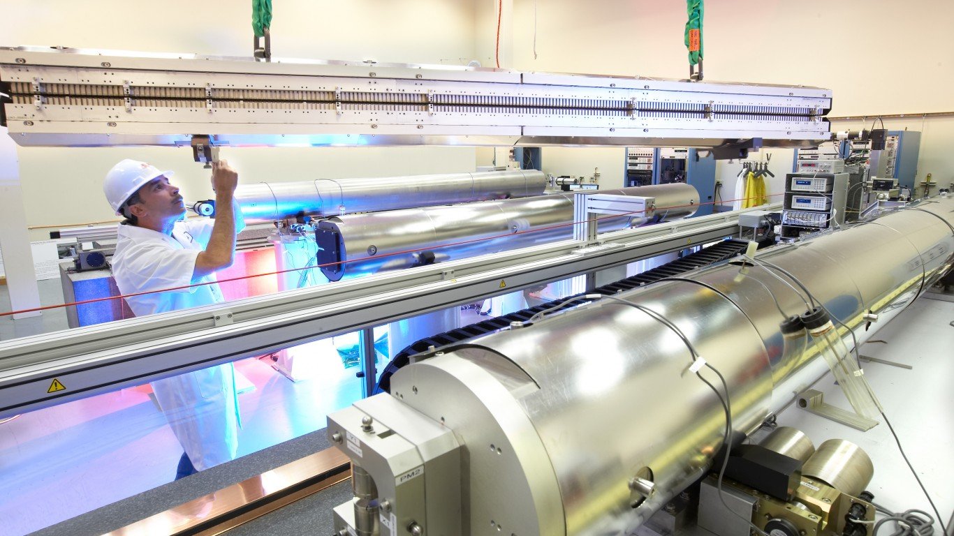

KLA (KLAC) is not like other semiconductor equipment companies, and that difference is becoming more important as AI drives a shift in how chips are manufactured. Specifically, KLAC primarily designs and sells “metrology and inspection” equipment. These are very different from the “processing” equipment from companies including Applied Materials (AMAT), Lam Research (LRCX), or Tokyo Electron (TOELY).
This distinction is becoming more important as semiconductor manufacturing shifts away from a model driven primarily by wafer volume and toward one increasingly defined by process complexity. Processing equipment suppliers scale with wafer starts, but metrology and inspection scale with the number of process steps, tighter tolerances, and the rising cost of yield loss.
Importantly, KLA’s equipment plays a crucial role in yield enhancement for semiconductor manufacturing. Its inspection systems can detect and classify defects at various stages of production, allowing manufacturers to identify and address issues that could impact yield. KLA’s advanced analytics and data management software help in analyzing the collected data to optimize process parameters and improve overall yield.
As a result, metrology and inspection are no longer secondary steps, but central to determining whether a wafer is economically viable. This role is expanding as AI-driven devices increase the economic value of each wafer. Advanced logic, HBM stacks, and next-generation DRAM nodes operate with extremely tight overlay and line-width tolerances.
At advanced nodes, a single defect can scrap an entire wafer or reduce the value of a high-performance device downstream. That shifts spending priorities. Yield is no longer an efficiency metric—it is a revenue metric. Companies will spend on inspection and metrology to protect output, not to optimize it.
Advanced Nodes and Wafer Pricing
For example, according to my report entitled Global Semiconductor Equipment: Markets, Market Share, Market Forecasts, which can be previewed on my website at The Information Network, A TSMC logic wafer at 3nm costs approximately $21,760 and contains on the order of 650 dies, while a 5nm wafer costs approximately $13,540 with roughly 750 dies. The loss of a standard 25-wafer cassette due to a process defect therefore translates into a loss of approximately $544,000 at 3nm versus $338,500 at 5nm. Chart 1 illustrates the trend in wafer price between 180 – 3nm.

Chart 1
For the most recent quarter, KLA’s results reflect this shift. The company is not benefiting from higher wafer starts, but from a greater number of inspection and measurement steps per wafer. As device complexity increases, customers are adding process control steps rather than simply adding capacity. That is why KLA’s revenue holds up even when broader wafer fab equipment spending becomes uneven.
Dominance in Metrology And Outperforming Peers
According to Table 1, KLA increased its share of metrology and inspection from 72.6% in 2024 to 73.8% in 2025. This gain reflects tightening overlay requirements and increasing mask complexity at advanced nodes.
Chart 2, illustrates the data in Table 1, showing KLA’s had a 73.8% share of the Metrology/Inspection market. Compared to top three competitors, the largest share of a competitor was Applied Materials with a 9.8% share in 2025, which incidentally was down from 11.1% in 2024. In fact, KLA’s dominance is evident in that every major competitor lost share in 2025.
Chart 2
According to Table 2, the global metrology and inspection market expanded from $6.0 billion in 2020 to $12.9 billion in 2025. This doubling reflects the need for increasing process complexity at advanced nodes, particularly in logic and memory tied to AI workloads. KLA’s revenue growth outpaced the market, indicating that it is capturing a disproportionate share of incremental spending.
Investor Takeaway
KLA holds a commanding position in the process control segment of the wafer fabrication equipment (WFE) industry, boasting a market share that is more than four times larger than its nearest competitor, Applied Materials.
This dominance is bolstered by the increasing complexity of semiconductor chips, which necessitates advanced process control solutions. As the industry shifts toward sophisticated architectures like chiplet-based designs, gate-all-around transistors, and high-bandwidth memory, the demand for KLA’s specialized equipment is expected to grow significantly.
The central focus of KLAC’s technology and products, as detailed above, is that by monitoring by inspection and metrology equipment, the more than 700 steps over three months to process a semiconductor wafers and device.
Importantly, KLA’s equipment plays a crucial role in yield enhancement for semiconductor manufacturing. Its inspection systems can detect and classify defects at various stages of production, allowing manufacturers to identify and address issues that could impact yield. KLA’s advanced analytics and data management software help in analyzing the collected data to optimize process parameters and improve overall yield.
Contact [email protected] for any questions or corrections.