
The semiconductor industry is one of the most advanced and complex in the world. The semiconductor industry relies on highly specialized supply chains and manufacturing equipment. This ecosystem becomes highly complex because advanced chip manufacturing requires many process steps. The process involves companies from all over the world. Since the sector requires atomic precision, the semiconductor equipment companies specialized in only a few manufacturing steps. Those companies continuously invest in their R&D departments to keep up with Moore’s law advances. The most dynamic segments are tooling and manufacturing equipment for the manufacturing facilities. The equipment can be categorized into several subsectors. The most relevant are etching, deposition, and lithography equipment. The companies involved in these processes are not true monopolies, but they benefit from strong competitive moats, and limited competition due to the complexity and sophistication of their technology.
Etching
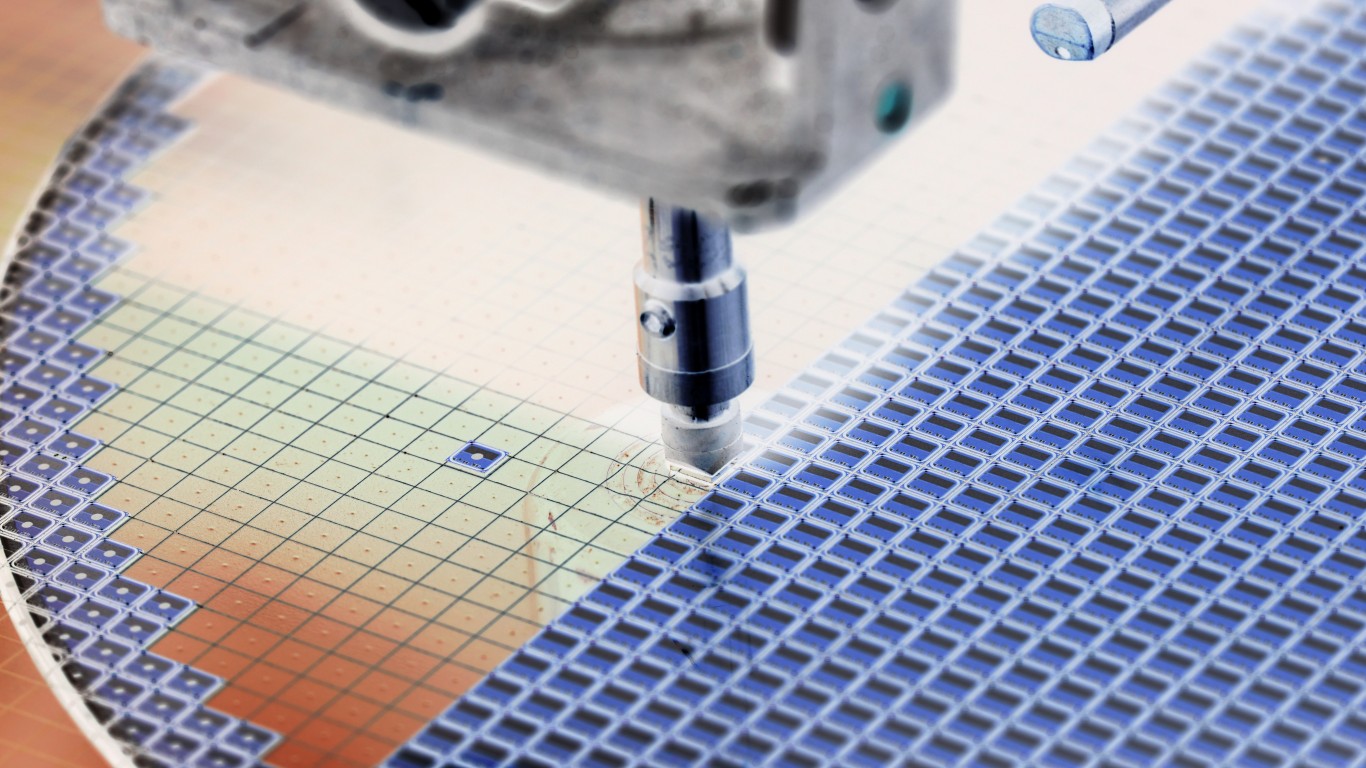
Etching is the process of engraving the complex lithographic designs into the silicon wafer. Traditionally, etching techniques relied on chemical processes, but the standard is now using plasma as the etchant. Normally, engineers place the patterns to be removed on the wafer using a lithographic mask over a photoresist. Then, the etchant removes the selected photoresist material from the wafer.
Lam Research (LRCX)
Lam is a global leader in wafer fabrication equipment and services, and advanced foundries use its machinery extensively. Most of its clients are located in Asia. In fact, TSMC, Samsung, SK Hynix, Micron, all use Lam Research equipment. Lam Research’s equipment centers around the etching processes but also interacts with different layers of the semiconductor manufacturing process, including deposition, cleaning and electroplating. Lam Research’s machinery supports current and future transistor architectures. For instance, Its Akara line is designed to surpass current industry etching needs. It is designed with future architectures in mind, including the early adoption of the CFET transistor node architecture, expected to go into production by 2030. Moreover, the company also provides advanced solutions for the memory industry and multichip architectures, including TSV and advanced high-aspect-ratio etching used by HBM memory and 3D NAND.
Next-generation nodes and Etching
Lam’s equipment is critical for the advanced nodes manufacturing both in logic and memory nodes. As Moore’s law demands processing power to double every 24 months, transistors must continue shrinking.
Logic Nodes
Up until 2022, the most advanced nodes relied on the FinFET transistor nodes. The current trend relies on GAAFET, also known as Gate All Around Transistor. TSMC pioneered the technology, and Samsung and Intel soon adopted it as well. This technology has enabled transistors in the 3 nm and down to 1.4 nm range. The next generation is the CFET, a combination of GAAFET transistors and 3D stacking techniques which is expected to enter production by 2030. This generation is expected to enable transistor technology up to 2 armstrongs or 0.2 nm.
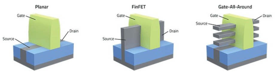
Transistor architecture evolution
This kind of technology relies heavily on etching processes and metal deposition, where Lam Research’s products dominate. In fact, it is this vertical stacking of transistors that makes etching technologies extremely critical. Indeed, the atomic layer deposition of material and the removal of these materials, determine yield, performance, and interconnect reliability of the logic. Indeed, the next major leap in semiconductor fabrication will center on 3D structures, a transition that depends heavily on advanced etching and deposition techniques.
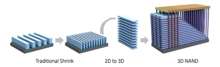
Memory architecture evolution
Memory Nodes
Lam claims that its last generation solid-state plama is unique in the industry, and allows 100x faster response to previous generations. Moreover, the company declares that in the 3D era of chips, EUV and advanced etching are critical for patterning and forming complex 3D structures and sub-nanometer scale. The memory industry is also evolving to different memory nodes including 3D NAND, 6F DRAM, 4F DRAM and 3D DRAM all of which require new etching technologies.
TSVs and Die to Die technology
In addition, Lam’s etching tools enable the precise fabrication of TSVs (Through Silicon Vias), which are essential for the next-generation chip architectures. The TSVs are essentially vertical structures that function as vias to connect different levels within the chip structure. For instance, these vias connect the logic and power distribution. This technology is essential for the CFET, and next generation chip architectures such as Intel’s Backside power delivery. Moreover, TSVs also allow for advanced chip packaging, as the industry is moving to transistor and memory cells 3D stacking, which is also the case for multichip packaging.
The so-called die-to-die, allows different silicon chips to be stacked on top of one another, in fact DRAM chips stacked this way also are referred to as HBM, like those produced by Micron. These chips allow manufacturers to produce complex structures modularly. In the case of HBM it is easier to manufacture multiple DRAM chips, known as chiplets, and stack them together than it is to create a monolithic chip with the characteristics of HBM. These kind of structures can only be manufactured with TSVs and advanced material deposition techniques, such as Lam’s.
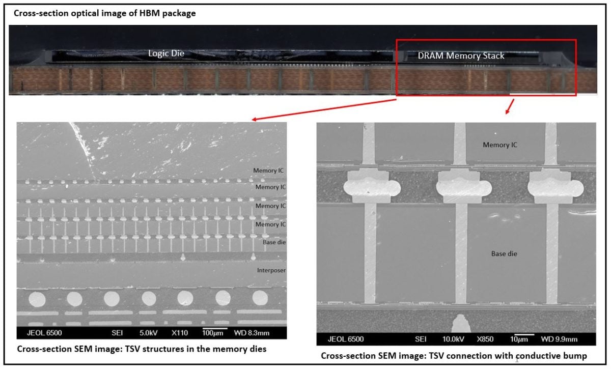
TSV and HBM memory
Beyond manufacturing equipment
Lam has identified that as the speed of computers doubles with Moore’s law, so does the complexity in manufacturing semiconductors. The so-called Lam’s law describes this principle. For instance, to manufacture a sub 5 nm node, there are over 100 trillion possible combinations. In order to sustain Moore’s law, Lam’s proposal includes several products: digital twins, virtual process simulation and smart tools.
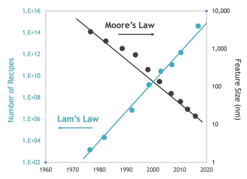
Lam’s Law
Lam Research’s digital twin approach allows manufacturers to create a virtual replica of the machine, enabling them to instantly test millions of process scenarios in software without wasting expensive physical silicon. On the other hand, its virtual simulation approach replaces the trial-and-error testing on real wafers and instead uses physics-based approaches to simulate plasma behavior. This enables the refinement of the manufacturing recipe in a digital environment before going into production. Finally, its smart tools continuously monitor equipment performance by actively calibrating sensors, system configurations, and process parameters in real time. This enables manufacturers to adjust processes on the fly, reducing optimization timelines from weeks to days.
Lam Research earnings and the current state of the company
In the last earnings report from Q1 FY26, the financial performance strongly supports this narrative. To illustrate, the company states that AI buildout is increasing the semiconductor manufacturing complexity, with Lam being a direct beneficiary. The management team believes AI will continue driving the semiconductor capex, specially in relation to memory and advanced logic nodes. Actually, the company stated that both chip demand and complexity will increase. For FY26, the company expects the Wafer Fab Equipment expenditure to increase to $140B, representing a 27% YoY growth.
For Q1, its revenue was around $5.84B with gross margins of 50% and operating margins of 35%. The next quarter guidance is also strong expecting around $6.6B, or 13% QoQ growth. On the other hand, the company also faces significant risks due to its heavy exposure to the Chinese market, which accounts for 34% of its revenue, while the broader Asian region represents nearly 90% of its business. For Lam Research, the four major trends driving business growth are NAND, DRAM, Logic, and Advanced Packaging. The company positions itself for multi-year outperformance as the semiconductor industry transitions from traditional 2D scaling toward increasingly complex 3D architectures across logic, memory, and advanced packaging technologies.
Author’s opinion
While Moore’s law describes the approximate doubling of computing power each 24 months, so does Lam’s law with the manufacturing complexity. As semiconductor nodes advance, device architectures are becoming increasingly three-dimensional, driving a substantial increase in the aspect ratios required for critical features. This trend makes advanced etching technologies a key manufacturing challenge and a critical enabler for future nodes.
I believe Lam has a critical role in the current and future semiconductor manufacturing business. This is because Lam has the technology to keep up with the current and future manufacturing nodes amid increasing AI compute demand.
Contact [email protected] for any questions or corrections.